Atmospheric Plasma Simplifies Die-to-Wafer Bonding
We present a simple Die-to-Wafer bonding process enabled by atmospheric plasma, eliminating the need for complicated carrier wafers and costly vacuum plasma systems. Applications include heterogeneous 3DIC and integrated photonics.
Link to Technical Paper:
Cleaning of Silicone and Hydrocarbon Contact Residue Using Atmospheric Plasma
Contact residue from dicing tape and silicone gel trays can cause poor adhesion in chip and wafer bonding applications. ONTOS atmospheric plasma is used to clean surfaces prior to bonding.
Metallurgy, Surface Preparation and Bonding for Cryogenic and Superconducting Hybrid Applications
This Paper by the Quantum Computing groups at Google and UCSB describes the materials and processes (including SET hybrid bonders and Ontos Atmospheric Plasma) which are now routinely used to produce leading-edge quantum computing components operating at superconducting temperatures.
Qubit compatible superconducting interconnects
- Manuscript (IOP website)
- Quantum supremacy – Google video
Evaluating Surface Wettability for SET-NA Ontos7 Atmospheric Plasma Treated Samples
This technical paper, published with the kind permission of ULTRA Communication, presents the wetting evaluation results of Surface Preparation using the ONTOS Atmospheric Plasma System
Evaluating Surface Wettability for Ontos Ontos7 Treated Samples
Utilization of Atmospheric Plasma Surface Preparation To Improve Copper Plating Processes
Many process steps in semiconductor manufacturing and packaging benefit from pristine surface preparation, such as descuming of photoresist, removal of native oxides, and surface activation. One particularly important surface process is the preparation of surfaces prior to copper plating.
ESTC 2016 publication, re-posted with the Authorization of IEEE.
Interconnect Structure for Room Temperature 3D-IC Stacking employing Binary Alloying for High Temperature Stability
We propose depositing Ni\In onto the Cu post on one side of the bond interface, and Ni\Ag to the other side to create a metallurgical system which can be bonded at room temperature to create robust mechanical and electrical interconnects. An Atmospheric Plasma process is used to de-oxidize and passivate the In and Ag surfaces, followed by room temperature compression bonding of the In to Ag. Subsequent chip layers can be stacked in the same manner at room temperature without requiring thermal excursions for melting and solidification. Following completion and test of the stacked assembly, solid-state annealing will alloy the In and Ag layers, raising the melt temperature of the In/Ag alloy to above standard solder assembly temperatures.
ESTC 2016 publication, re-posted with the Authorization of IEEE.
Characterization of a Novel Fluxless Surface Preparation Process for Die Interconnect Bonding
For applications such as 3D integration, flip chip, and other die interconnection processes, a variety of metals is used to form an electrical and mechanical bond between the two components.
ECTC 2012 publication, re-posted with the Authorization.
AU Bonding
An unexpected bonding benefit was discovered while bonding Gold pads to Gold pads for a flip-chip configuration. Low-temperature compression bonding (necessitated by chip temperature restrictions to 200C) had yielded very poor adhesion between Gold pads, even though there was significant visual pad-to-pad compression.
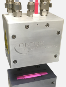
Competitive Advantages of Ontos7 Atmospheric Plasma
This document highlights the Advantages of Ontos7 Atmospheric Plasma Process over Vacuum RIE Plasma for Die/Wafer Surface Preparation, and over Competitive Atmospheric Plasma Products for the Preparation of Semiconductor Surfaces.
Multifunctional integrated photonics in the
mid-infrared with suspended AlGaAs on silicon
The microscale integration of mid- and long-wave-infrared photonics could enable the development of fieldable,
robust chemical sensors, as well as highly efficient infrared frequency converters. However, such technology would
be defined by the choice of material platform, which immediately determines the strength and types of optical non-
linearities available, the optical transparency window, modal confinement, and physical robustness. In this work, we
demonstrate a new platform, suspended AlGaAs waveguides integrated on silicon, providing excellent performance in
all of these metrics.
Multifunctional integrated photonics in the mid-infrared with suspended AlGaAs on silicon: supplementary material
This document provides supplementary information to “Multifunctional integrated photonics in
the mid-infrared with suspended AlGaAs on silicon,”
Infrared frequency comb generation and
spectroscopy with suspended silicon nanophotonic
waveguides
Nanophotonic waveguides with sub-wavelength mode confinement and engineered dispersion are an excellent
platform for application-tailored nonlinear optical interactions at low pulse energies. We present fully air-clad sus-
pended silicon waveguides for infrared frequency comb generation with optical bandwidth limited only by the silicon
transparency.
Infrared frequency comb generation and spectroscopy with suspended silicon nanophotonic waveguides: supplementary material
This document provides supplementary information to “Infrared frequency comb generation and
spectroscopy with suspended silicon nanophotonic waveguides.” This document contains four sections. Section 1 explains the details of the suspended Si
waveguides fabrication. Section 2 gives a detailed explanation of the generalized nonlinear
Schrödinger equation used to model the generated supercontinuum spectra at different waveguide
widths. Section 3 explains the baseline fitting and subtraction to study dual-comb measured
atmospheric water absorbance data. We also explain the detailed procedure for the comparison of the
data with HITRAN database to estimate the experimental atmospheric pressure and water content.
Section 4 provides the detailed process for background subtraction of the broadband liquid-phase dual-
comb data. Section 5 goes through the detailed spectral peak assignments of the measured vibrational lines
in DCS of isopropanol and methanol.
Efficient second harmonic generation in
nanophotonic GaAs-on-insulator waveguides
Here we demonstrate
second harmonic generation (SHG) in GaAs-on-insulator waveguides with unprecedented
efficiency of 40 W−1
for a single-pass device.
Qubit compatible superconducting interconnects
We present afabrication processforfully superconducting interconnects compatiblewith superconducting
qubit technology. These interconnects allowfor the three dimensional integration of quantum circuits
without introducing lossy amorphous dielectrics.