With oxidizing chemistry, ONTOS can passivate sensitive semiconductor surfaces without damaging them, and can prepare ultra-clean, ultra-activated surfaces for direct bonding: die-to-die, die-to-wafer, or wafer-to-wafer.
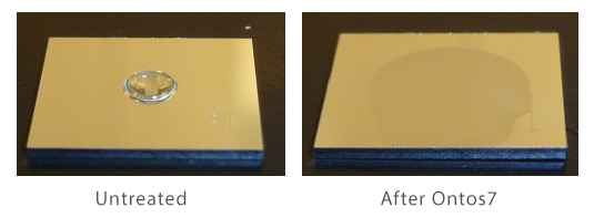
ONTOS Atmospheric Plasma also produces highly activated surfaces for improved wetting, wicking, and adhesion. Activation has been demonstrated on Sn, Ag, Cu, Au, In, Ni, Al, Ti, Si, SiO2, Si3N4, Al2O3, photoresist, and FR composites.
The contact angle photos below for Tin-Silver are typical for all of the materials we have tried to date:
Get the Download!
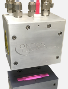
ONTOS is used for many applications within the semiconductor industry for Surface Preparation using a uniquely designed, patented Atmospheric Plasma with oxidizing or reducing chemistry. ONTOS:
- Performs Cleaning
- Eliminates Organic Contamination
- Activates Surfaces
- Removes Oxidation
Our innovative process applies a gaseous passivation that delays the re-oxidation of the metallic surfaces. Learn more about the process and where ONTOS is used!