Wafer Level System Integration
The department "Wafer Level System Integration" (WLSI) develops advanced packaging and system integration technologies and offers customer-specific solutions for microelectronic products in the overall scope of smart system integration. Approx. 60 scientists work at two locations: Berlin and Dresden (ASSID: All Silicon System Integration Dresden). WLSI is cooperating globally with manufacturers and users of microelectronic products as well as cleanroom equipment producers and material developers from the chemical industry.
Wafer Level Packaging Line
800 m² clean room (classes 10 to 1000) + 800 m² gray room, 4’’, 6’’ and 8’’, prototyping equipment for some applications also on 300 mm
- Thin-film deposition
- Photolithography (including photo varnishes, polymers and spray coating)
- Galvanic bumping, circuit tracks and through-via filling (Cu, Ni, Au, AuSn, SnAg, PbSn)
- Wet-chemical processes (etching, cleaning)
- Wafer bonding (support wafer, thin-wafer handling)
- Silicon plasma etching (through vias, cavities)
For information about booking a demonstration, please contact:
Gilbert Lecarpentier
glecarpentier@ontosplasma.com
+33 0-671-84-69-71
CERTeM : Microelectronics Technological Research and Development Center
CERTeM is a public/private collaborative research group in the field of microelectronics. Thanks to its skills and equipment, CERTeM offers innovative solutions in the field of energy efficiency. CERTeM has state-of-the-art technological platforms for R&D projects of its members and their partners, as well as start-ups developing innovative materials and devices.
CERTeM's activities cover three main research topics :
- Energy efficiency of electrical systems
- Integrated systems for mobile electronics
- Energy micro-sources
Since several years, CERTeM is involved in a transversal research topic : interconnexion and packaging of 3D components. In 2014 CERTeM has developed a platform entirely dedicated to interconnection, packaging and advanced characterization : CERTeM + .
For information about booking a demonstration, please contact:
Gilbert Lecarpentier
glecarpentier@ontosplasma.com
+33 0-671-84-69-71
Boulder Microfabrication Facility
Central to fulfilling many of the Division’s programmatic goals, and those of other divisions at NIST-Boulder, the Quantum Electromagnetics Division is responsible for operation of the state-of-the-art Boulder Microfabrication Facility (BMF).
The Boulder Microfabrication Facility (BMF) is a 1700 m2 (18,000 ft2), ISO class 5 (class 100) clean room dedicated to providing state-of-the-art micro- and nano-fabrication capabilities to meet the microelectronic and microelectromechanical systems needs of NIST-Boulder staff members and their direct collaborators. Roughly 60 % of all the research on site passes through the BMF in one critical way or another.
Quantum Sensors Group
The Quantum Sensors Group, part of NIST’s Physical Measurement Laboratory, and the Quantum Electromagnetics Division, advances the detection of photons and particles in a variety of application areas using superconducting sensors and readout electronics.
The Group focuses on:
- quantum effects, including superconductivity;
- low temperatures to reduce thermal noise; and
- the development of advanced sensors.
Major activities of the Group include:
- superconducting x-ray and gamma-ray spectrometers for applications that include materials analysis and nuclear materials accounting
- superconducting microbolometers for applications that include concealed weapons detection and understanding the early universe
- advanced cryogenics to aid the dissemination of cryogenic sensors
- the determination of x-ray fundamental parameters to facilitate materials analysis by x-ray techniques
- support of U.S. industries that develop or use advanced cryogenics and cryogenic sensors
For information about booking a demonstration, please contact:
Jeffrey Friot
jfriot@ontosplasma.com
+1 802-522-0898
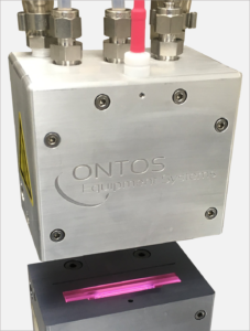
ONTOS Equipment Systems Demonstration/Prototyping Lab is strategically located in the heart of the Green Mountains of Vermont. ONTOS Equipment Systems prides itself in supporting technological innovation and encouraging collective activity between industries and research and development institutions. It concentrates on supporting new and emerging companies and their subsidiaries in all semiconductor sectors.
Our laboratory offers:
- Experienced engineering and technical staff
- Cost-effective alternative to investing in capital equipment
- Controlled heating and cooling systems
- ISO Class 4 cleanroom
- Secure material storage
- Strict IP confidentiality
- Various measurement systems available for characterization
- High accuracy/High force Flip Chip device bonder
For information about booking a demonstration, please contact:
Jeffrey Friot
jfriot@ontosplasma.com
+1 802-522-0898