ONTOS
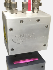
ONTOS is an atmospheric plasma system for surface preparation. Our patented equipment and processes provide unique advantages to our customers. Key benefits of our atmospheric plasma tools include:
- Low-cost, high yield, high-speed, chip-to-chip interconnect bonds at room temperature with minimal force
- Better surface activation for direct bonding, aqueous wetting, contamination removal, and adhesive bonding
Features
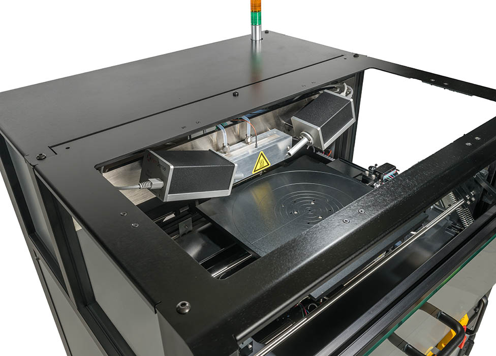
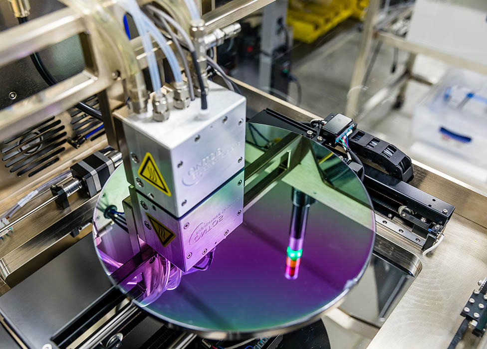
- Chip/wafer is scanned under compact process head
- Plasma-Head selection: 25mm, 40mm or 100mm wide (rastered)
- Typical scan rate: 1-5 mm/sec
- Process runs in room ambient
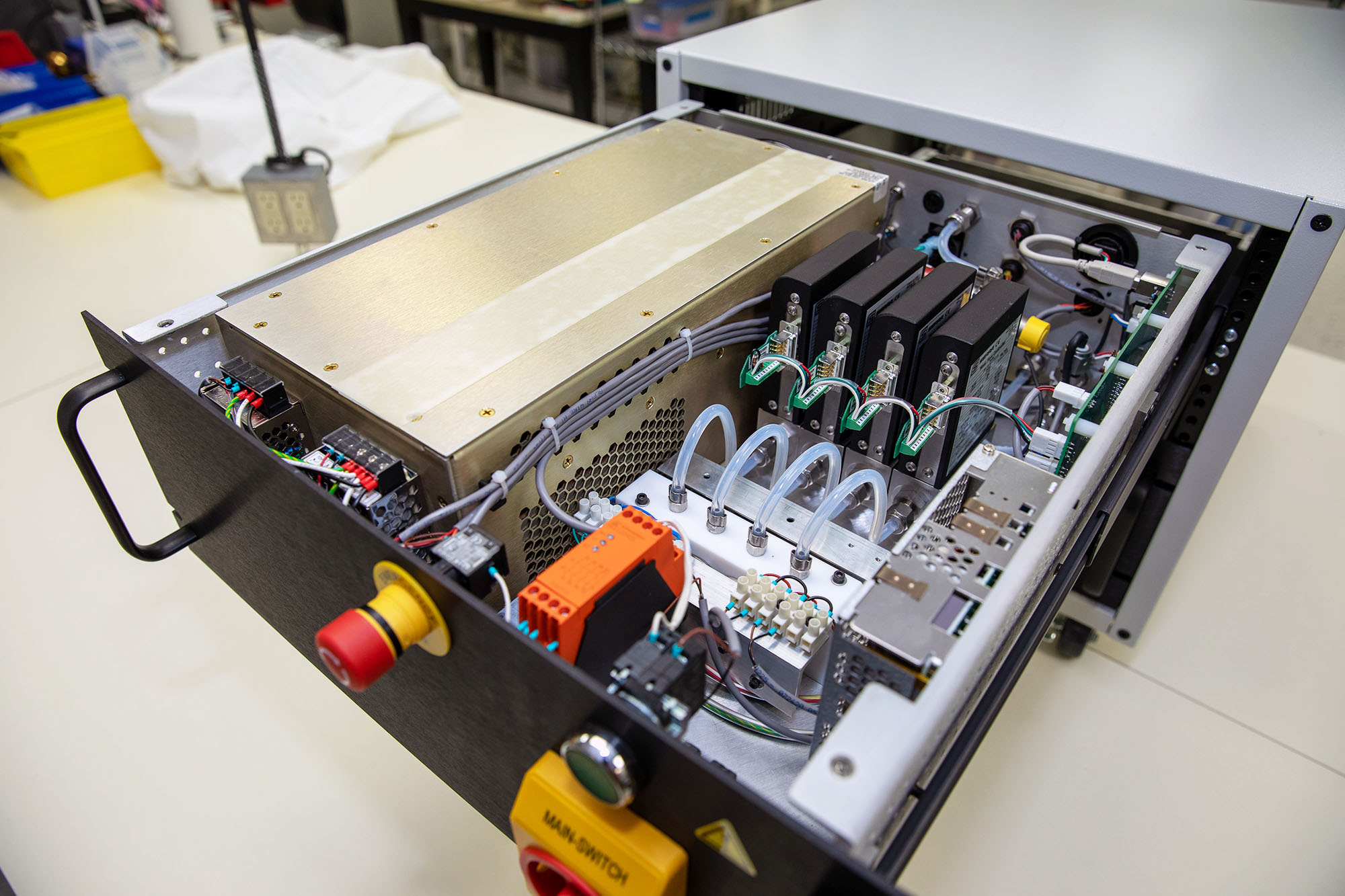
- Programmable control of plasma and scan parameters
- Easy touch-screen controller
- Vacuum chuck handles small chips to 8” wafers. (or 12″ wafer with the 300mm)
- Typical power to internal plasma source: 60-100 Watts
- CE certified (by independent third party)
- Made in U.S.A.
ONTOS Atmospheric Plasma Solutions
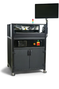
Semiautomated system for Surface Preparation using a patented Atmospheric Plasma with a unique design enabling, without any modification, oxidizing or reducing chemistry.
- Removes native oxide from metallic and semiconductor surfaces
- Engineered surface termination inhibits re-oxidation
- Removes residual organic contamination films
- Fast, non-toxic, dry, atmospheric process
- Low-energy surface chemistry – CMOS safe
- Ideal surface preparation for direct bonding
- Compact configuration
- Automation compatible
- Custom Chucks
Learn More
The OEM version of the ONTOS Plasma Head is available for integration into third party equipment.
The Plasma Curtain is available in several widths (down to 10mm) to enable optimization of the gas consumption on smaller devices or to adapt to larger devices.
Learn More
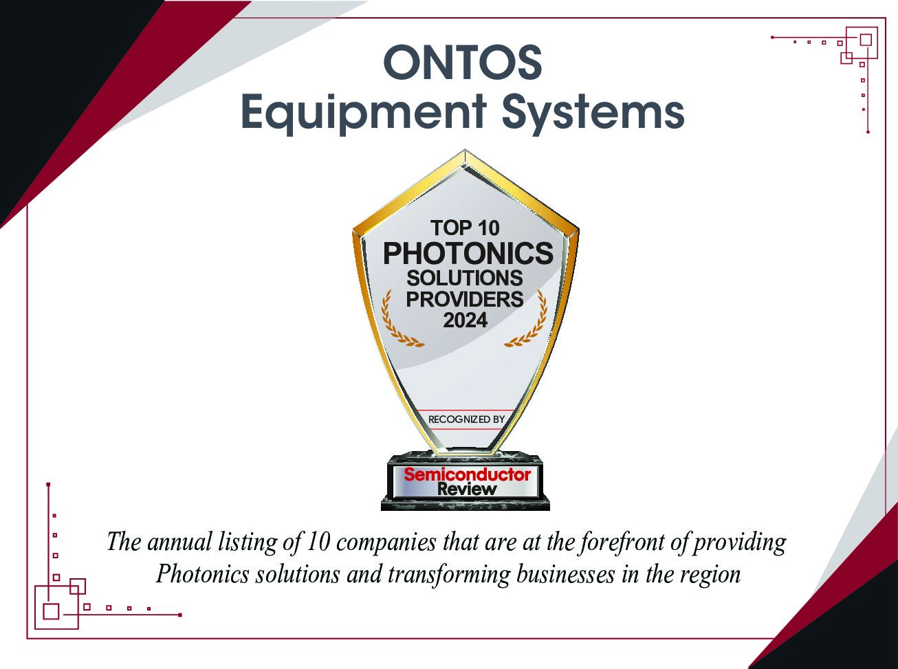
Click Here to see us on Semiconductor Review!